- 您现在的位置:买卖IC网 > Sheet目录3840 > PIC18F6410-I/PT (Microchip Technology)IC PIC MCU FLASH 8KX16 64TQFP
2010-2012 Microchip Technology Inc.
DS39977F-page 103
PIC18F66K80 FAMILY
6.1.2
PROGRAM COUNTER
The Program Counter (PC) specifies the address of the
instruction to fetch for execution. The PC is 21 bits wide
and contained in three separate 8-bit registers.
The low byte, known as the PCL register, is both
readable and writable. The high byte, or PCH register,
contains the PC<15:8> bits and is not directly readable
or writable. Updates to the PCH register are performed
through the PCLATH register. The upper byte is called
PCU. This register contains the PC<20:16> bits; it is also
not directly readable or writable. Updates to the PCU
register are performed through the PCLATU register.
The contents of PCLATH and PCLATU are transferred to
the Program Counter by any operation that writes PCL.
Similarly, the upper two bytes of the Program Counter
are transferred to PCLATH and PCLATU by an operation
that reads PCL. This is useful for computed offsets to the
PC (see Section 6.1.5.1 “Computed GOTO”).
The PC addresses bytes in the program memory. To
prevent the PC from becoming misaligned with word
instructions, the Least Significant bit (LSb) of PCL is
fixed to a value of ‘0’. The PC increments by two to
address sequential instructions in the program memory.
The CALL, RCALL, GOTO and program branch
instructions write to the Program Counter directly. For
these instructions, the contents of PCLATH and
PCLATU are not transferred to the Program Counter.
6.1.3
RETURN ADDRESS STACK
The return address stack enables execution of any
combination of up to 31 program calls and interrupts.
The PC is pushed onto the stack when a CALL or
RCALL
instruction is executed or an interrupt is
Acknowledged. The PC value is pulled off the stack on
a RETURN, RETLW or a RETFIE instruction. The value
is also pulled off the stack on ADDULNK and SUBULNK
instructions if the extended instruction set is enabled.
PCLATU and PCLATH are not affected by any of the
RETURN
or CALL instructions.
The stack operates as a 31-word by 21-bit RAM and a
5-bit Stack Pointer, STKPTR. The stack space is not
part of either program or data space. The Stack Pointer
is readable and writable and the address on the top of
the stack is readable and writable through the
Top-of-Stack (TOS) Special Function Registers. Data
can also be pushed to, or popped from the stack, using
these registers.
A CALL type instruction causes a push onto the stack.
The Stack Pointer is first incremented and the location
pointed to by the Stack Pointer is written with the
contents of the PC (already pointing to the instruction
following the CALL). A RETURN type instruction causes
a pop from the stack. The contents of the location
pointed to by the STKPTR are transferred to the PC
and then the Stack Pointer is decremented.
The Stack Pointer is initialized to ‘00000’ after all
Resets. There is no RAM associated with the location
corresponding to a Stack Pointer value of ‘00000’; this
is only a Reset value. Status bits indicate if the stack is
full, has overflowed or has underflowed.
6.1.3.1
Top-of-Stack Access
Only the top of the return address stack is readable and
writable. A set of three registers, TOSU:TOSH:TOSL,
holds the contents of the stack location pointed to by
the STKPTR register (Figure 6-3). This allows users to
implement a software stack, if necessary. After a CALL,
RCALL
or interrupt (or ADDULNK and SUBULNK instruc-
tions, if the extended instruction set is enabled), the
software can read the pushed value by reading the
TOSU:TOSH:TOSL registers. These values can be
placed on a user-defined software stack. At return time,
the
software
can
return
these
values
to
TOSU:TOSH:TOSL and do a return.
While accessing the stack, users must disable the
Global Interrupt Enable bits to prevent inadvertent
stack corruption.
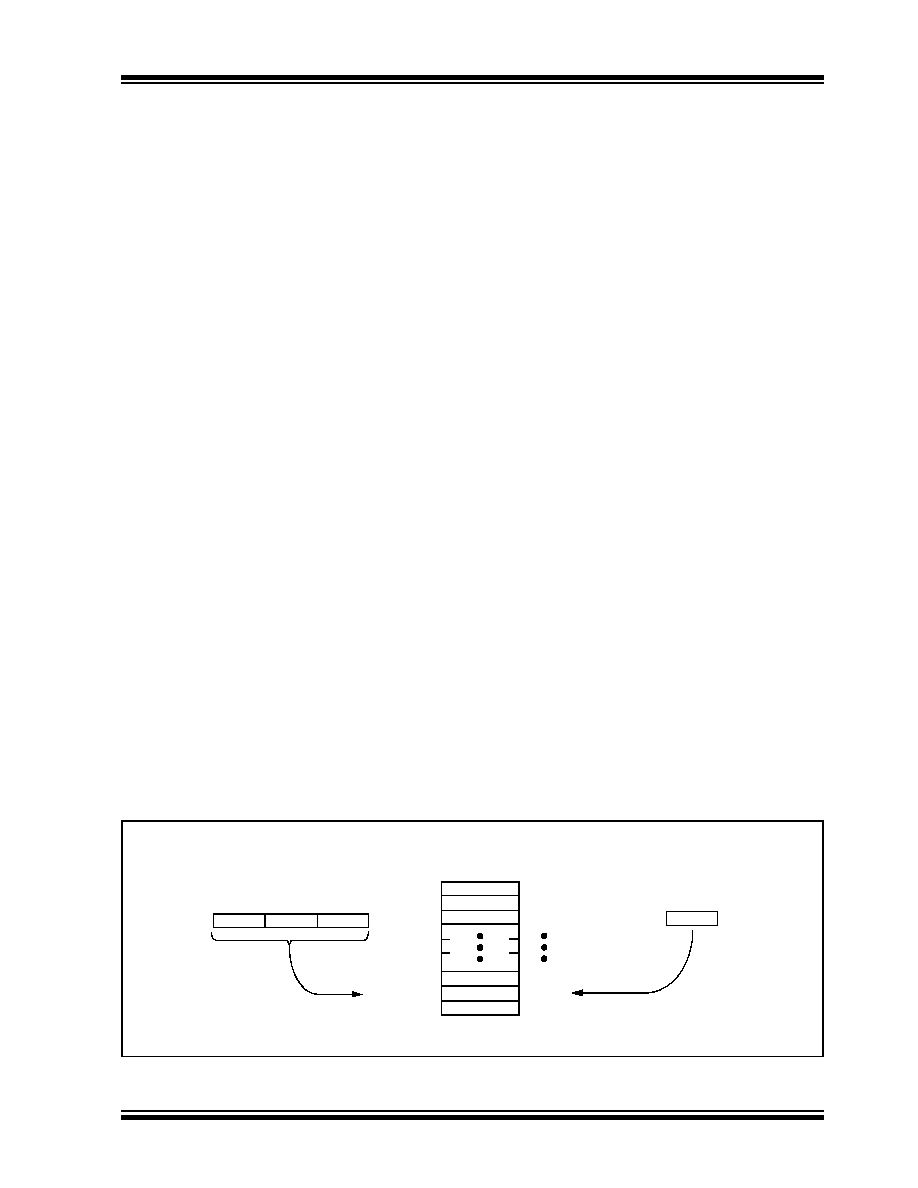
FIGURE 6-3:
RETURN ADDRESS STACK AND ASSOCIATED REGISTERS
00011
001A34h
11111
11110
11101
00010
00001
00000
00010
Return Address Stack<20:0>
Top-of-Stack
000D58h
TOSL
TOSH
TOSU
34h
1Ah
00h
STKPTR<4:0>
Top-of-Stack Registers
Stack Pointer
发布紧急采购,3分钟左右您将得到回复。
相关PDF资料
200346-2
CONN HOUSING RECEPT 20POS BLACK
PIC16F84A-20/P
IC MCU FLASH 1KX14 EE 18DIP
200838-2
CONN HOUSING RECEPT 34POS BLACK
PIC18LF2420-I/SO
IC MCU FLASH 8KX16 28SOIC
5172625-3
CONN RCPT HSNG 24POS BLUE PNL MT
202758-1
CONN HOUSING PLUG 6POS BLACK
TS80C31X2-VIC
IC MCU 8BIT 40/30MHZ 44-PQFP
TS80C31X2-MCC
IC MCU 8BIT 40/20MHZ 44-PQFP
相关代理商/技术参数
PIC18F6410-I/PT
制造商:Microchip Technology Inc 功能描述:IC 8BIT FLASH MCU 18F6410 TQFP64
PIC18F6410T-I/PT
功能描述:8位微控制器 -MCU 16kBF 768RM 68I/O RoHS:否 制造商:Silicon Labs 核心:8051 处理器系列:C8051F39x 数据总线宽度:8 bit 最大时钟频率:50 MHz 程序存储器大小:16 KB 数据 RAM 大小:1 KB 片上 ADC:Yes 工作电源电压:1.8 V to 3.6 V 工作温度范围:- 40 C to + 105 C 封装 / 箱体:QFN-20 安装风格:SMD/SMT
PIC18F6490-E/PT
功能描述:8位微控制器 -MCU 16kBF 768RM 68I/O RoHS:否 制造商:Silicon Labs 核心:8051 处理器系列:C8051F39x 数据总线宽度:8 bit 最大时钟频率:50 MHz 程序存储器大小:16 KB 数据 RAM 大小:1 KB 片上 ADC:Yes 工作电源电压:1.8 V to 3.6 V 工作温度范围:- 40 C to + 105 C 封装 / 箱体:QFN-20 安装风格:SMD/SMT
PIC18F6490-I/PT
功能描述:8位微控制器 -MCU 16kBF 768RM 68I/O RoHS:否 制造商:Silicon Labs 核心:8051 处理器系列:C8051F39x 数据总线宽度:8 bit 最大时钟频率:50 MHz 程序存储器大小:16 KB 数据 RAM 大小:1 KB 片上 ADC:Yes 工作电源电压:1.8 V to 3.6 V 工作温度范围:- 40 C to + 105 C 封装 / 箱体:QFN-20 安装风格:SMD/SMT
PIC18F6490-I/PT
制造商:Microchip Technology Inc 功能描述:IC 8BIT FLASH MCU 18F6490 TQFP64
PIC18F6490-I/PT
制造商:Microchip Technology Inc 功能描述:8 BIT MICROCONTROLLER CLOCK SPEED:40MHZ
PIC18F6490T-I/PT
功能描述:8位微控制器 -MCU 16kBF 768RM 68I/O RoHS:否 制造商:Silicon Labs 核心:8051 处理器系列:C8051F39x 数据总线宽度:8 bit 最大时钟频率:50 MHz 程序存储器大小:16 KB 数据 RAM 大小:1 KB 片上 ADC:Yes 工作电源电压:1.8 V to 3.6 V 工作温度范围:- 40 C to + 105 C 封装 / 箱体:QFN-20 安装风格:SMD/SMT
PIC18F6493-I/PT
功能描述:8位微控制器 -MCU 128 Segmnt LCD DRVR 12B ADC 16KB 768BRAM RoHS:否 制造商:Silicon Labs 核心:8051 处理器系列:C8051F39x 数据总线宽度:8 bit 最大时钟频率:50 MHz 程序存储器大小:16 KB 数据 RAM 大小:1 KB 片上 ADC:Yes 工作电源电压:1.8 V to 3.6 V 工作温度范围:- 40 C to + 105 C 封装 / 箱体:QFN-20 安装风格:SMD/SMT